Access to our latest beta chamber technology with comprehensive R&D licensing packages. Perfect for early adopters and research institutions seeking leading-edge solutions
Collaborative bespoke joint development projects tailored to your specific manufacturing requirements. Partner with us to integrate APS™ technology into your processes.
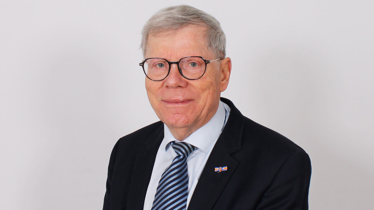
AlixLabs today announced the appointment of Arthur van der Poel to its Advisory Board, further strengthening the company’s strategic and technological leadership as it advances its semiconductor innovation roadmap.
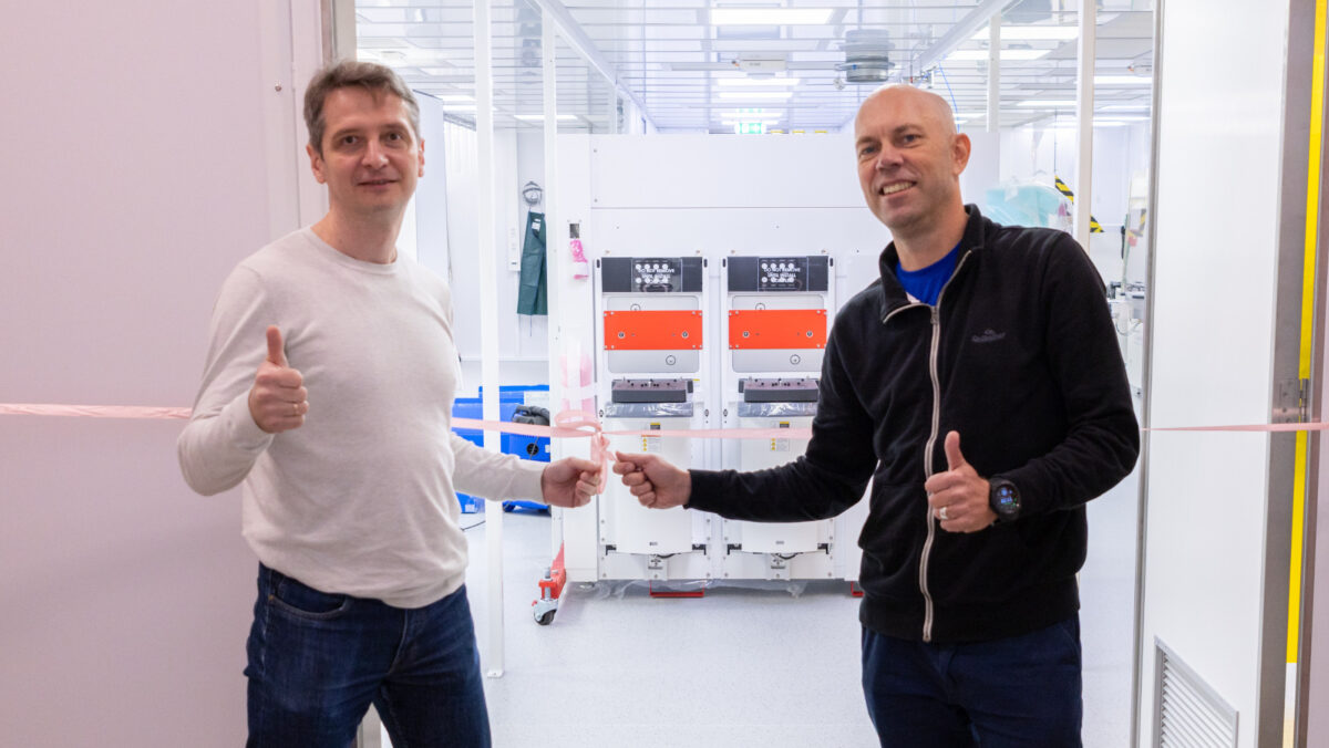
New automation platform paves way for fully automated, fab-ready solution for the company’s innovative, cost-effective and sustainable pitch splitting technology.
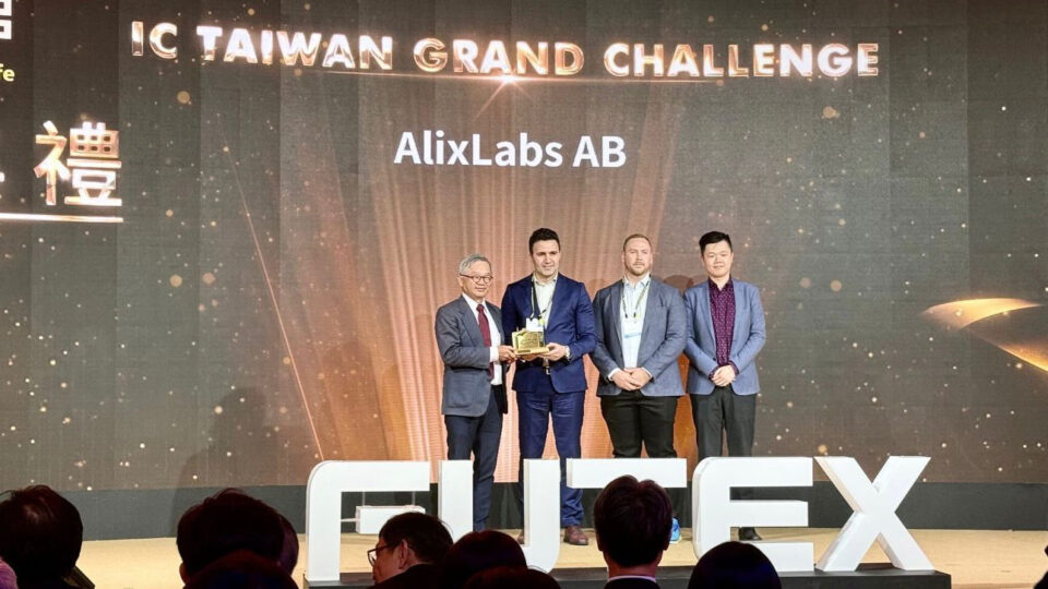
We are proud to announce that our innovative APS™ (Atomic Layer Etch Pitch Splitting) technology has been recognized with top honors at the IC Taiwan Grand Challenge, standing out among more than 150 international startups.
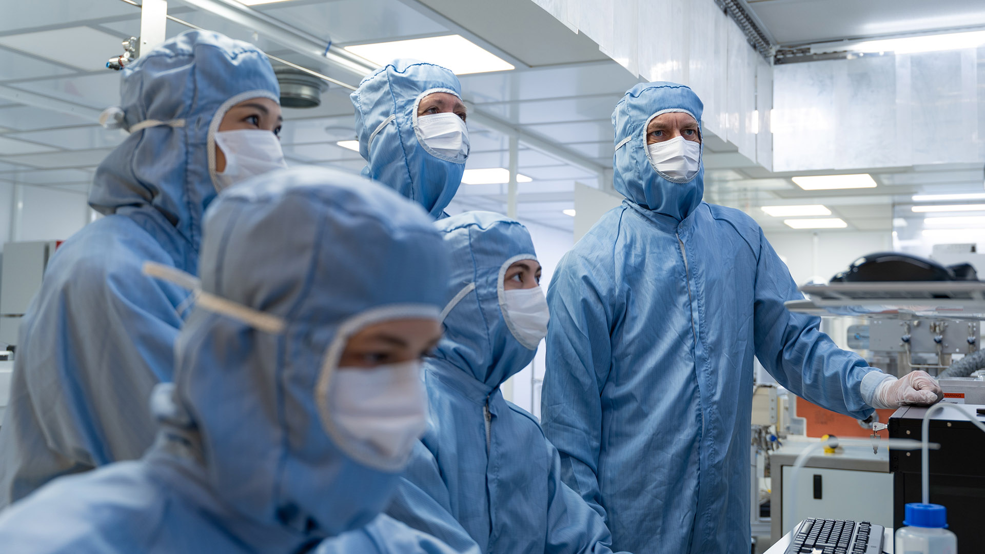
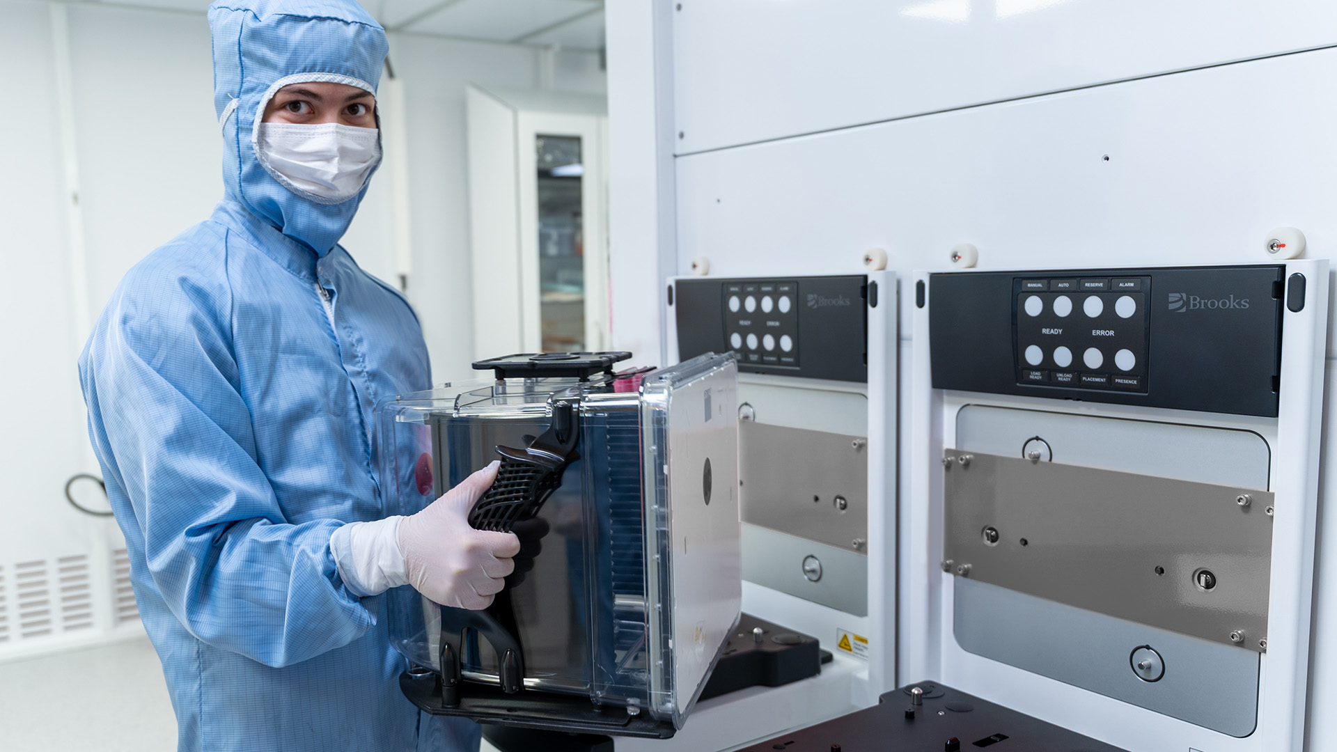
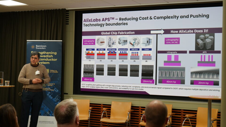
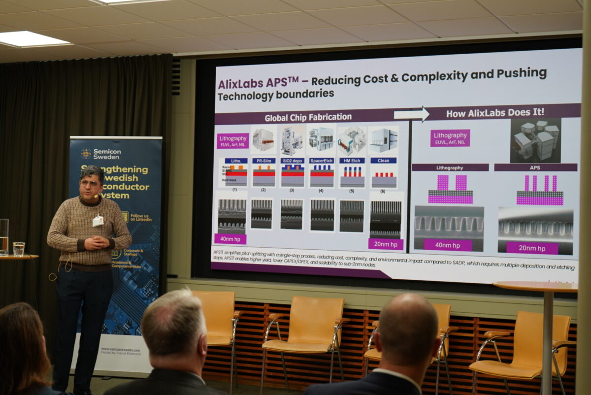
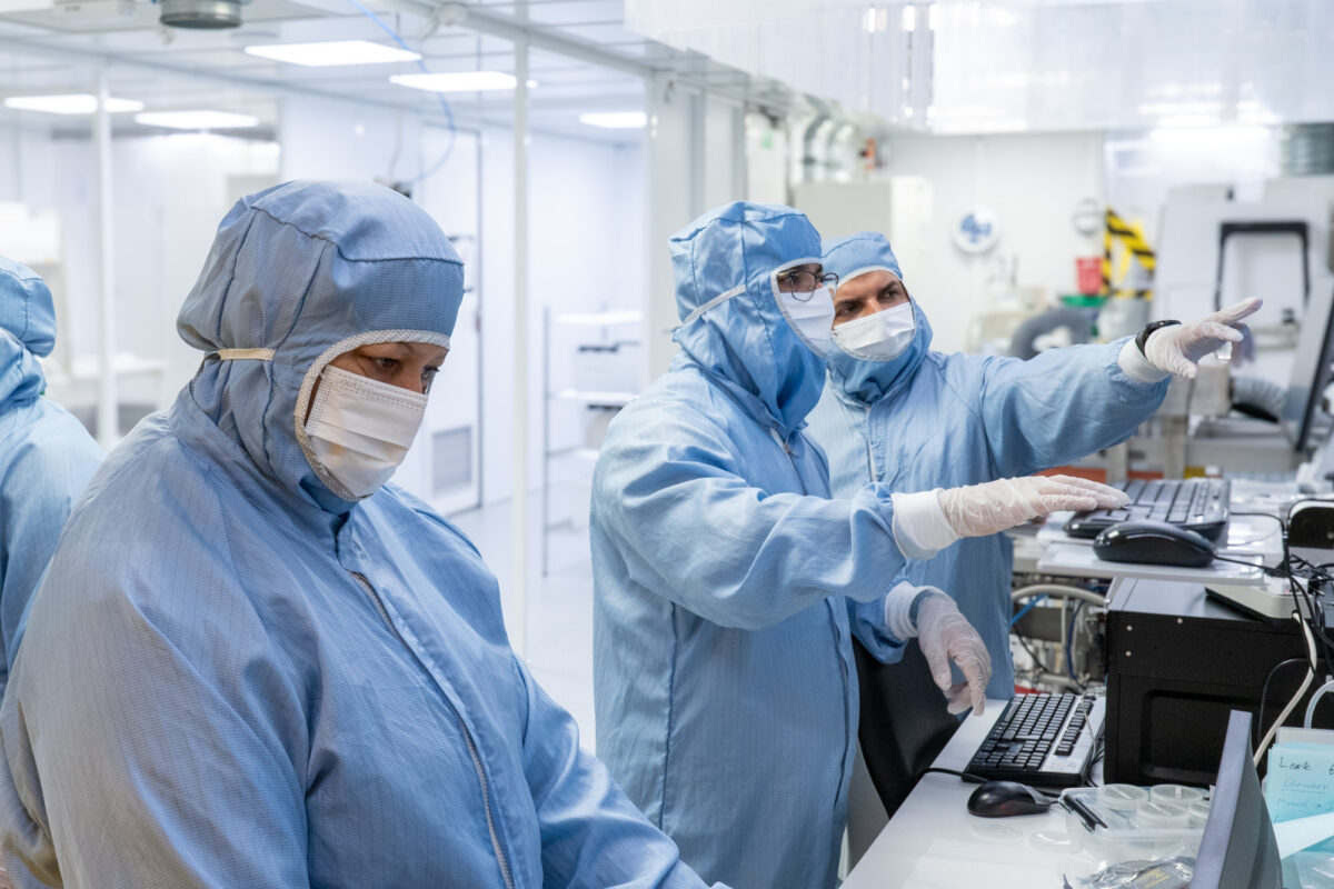
AlixLabs is a Swedish semiconductor industry supplier with equipment and processes capable of manufacturing nanostructures with characteristic sizes smaller than 20 nanometers.
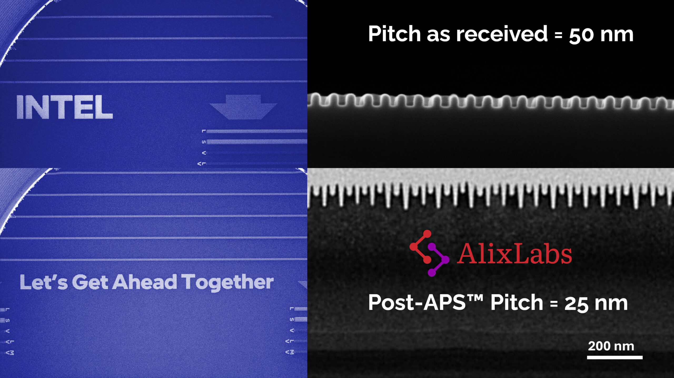
We enable energy efficient fabrication of structures beyond the resolution limits of optical and electron beam lithography – through APS™.


