

Swedish semiconductor startup to demonstrate 3-nanometer class FinFET structures made with APS™ on Intel Silicon at trade show.
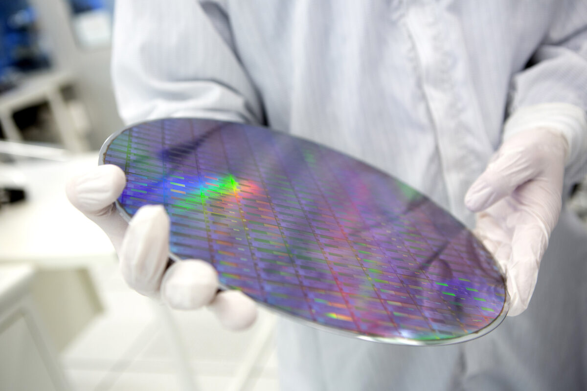
Stockholm, Sweden – February 7th, 2025 – AlixLabs AB, a Swedish semiconductor startup specializing in Atomic Layer Etching (ALE), announces that it has used its APS™ (ALE Pitch Splitting) technology to etch structures corresponding to commercial 3-nanometer semiconductor processes on test silicon provided by Intel. The results will be shared in full by CTO and co-founder Dmitry Suyatin at the SPIE Advanced Lithography + Patterning trade show in San Jose, California, 23–27 February.
“We are excited to demonstrate how APS™ can help the industry lessen its reliance on multi-patterning solutions in Silicon Valley, while lowering costs and environmental impact. Our tech has been able to produce sub-10-nanometer class features on silicon, and with the help of Intel’s Test Vehicle Program we have proven that sub-5-nanometer class features are possible on mass-production silicon by just etching,” says Dmitry Suyatin, CTO and co-founder of AlixLabs.
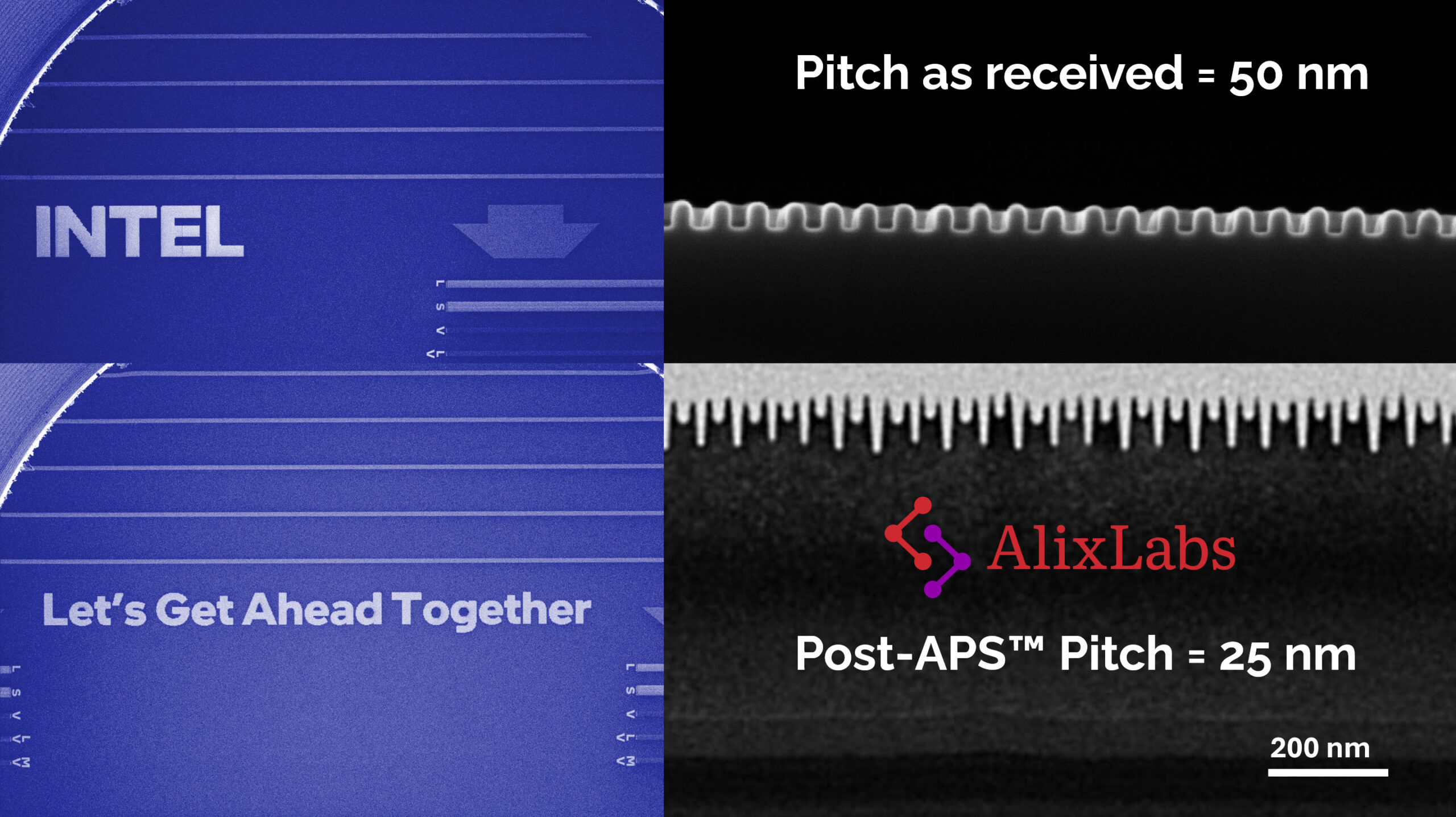
AlixLabs APS™ achieved a 25 nm full metal pitch, comparable to 3-nanometer class technology from the leading foundries, on the Intel Low Global Warming Potential Etch Test Vehicle. This is a major milestone on the company’s road to commercialization, with further news to follow later in 2025.
“APS™ proves that there’s no need for complex multi-patterning like SADP and SAQP to produce 5 nanometer chips and beyond. It extends the potential of immersion lithography for use with critical mask layers for even 3-nanometer processes,” says Jonas Sundqvist, CEO and co-founder of AlixLabs. “These results were produced with our alpha tool, with a beta tool to follow later in 2025. We wish to thank Intel for providing leading-edge grade test silicon for this demonstration.”
For more information on the latest APS™ developments at SPIE Advanced Lithography + Patterning, make sure to attend Dmitry Suyatin’s presentation on February 27th, at 9:00–9:20 AM (PST).

