


Atomic Layer Etching Pitch Splitting (APS) proven on more industry-leading wafers, doubling fin density and proving flexibility without EUV.
Austin, TX, USA/Stockholm, Sweden – April 10th, 2025 – AlixLabs AB, a Swedish semiconductor startup specializing in Atomic Layer Etching (ALE), today demonstrates the latest in its line of groundbreaking development in advanced chip fabrication unveiling additional research into its novel semiconductor manufacturing process known as APS™ (Atomic Layer Etching Pitch Splitting) capable of doubling fin density while introducing the unprecedented flexibility to vary pitch and critical dimensions within the same wafer area.
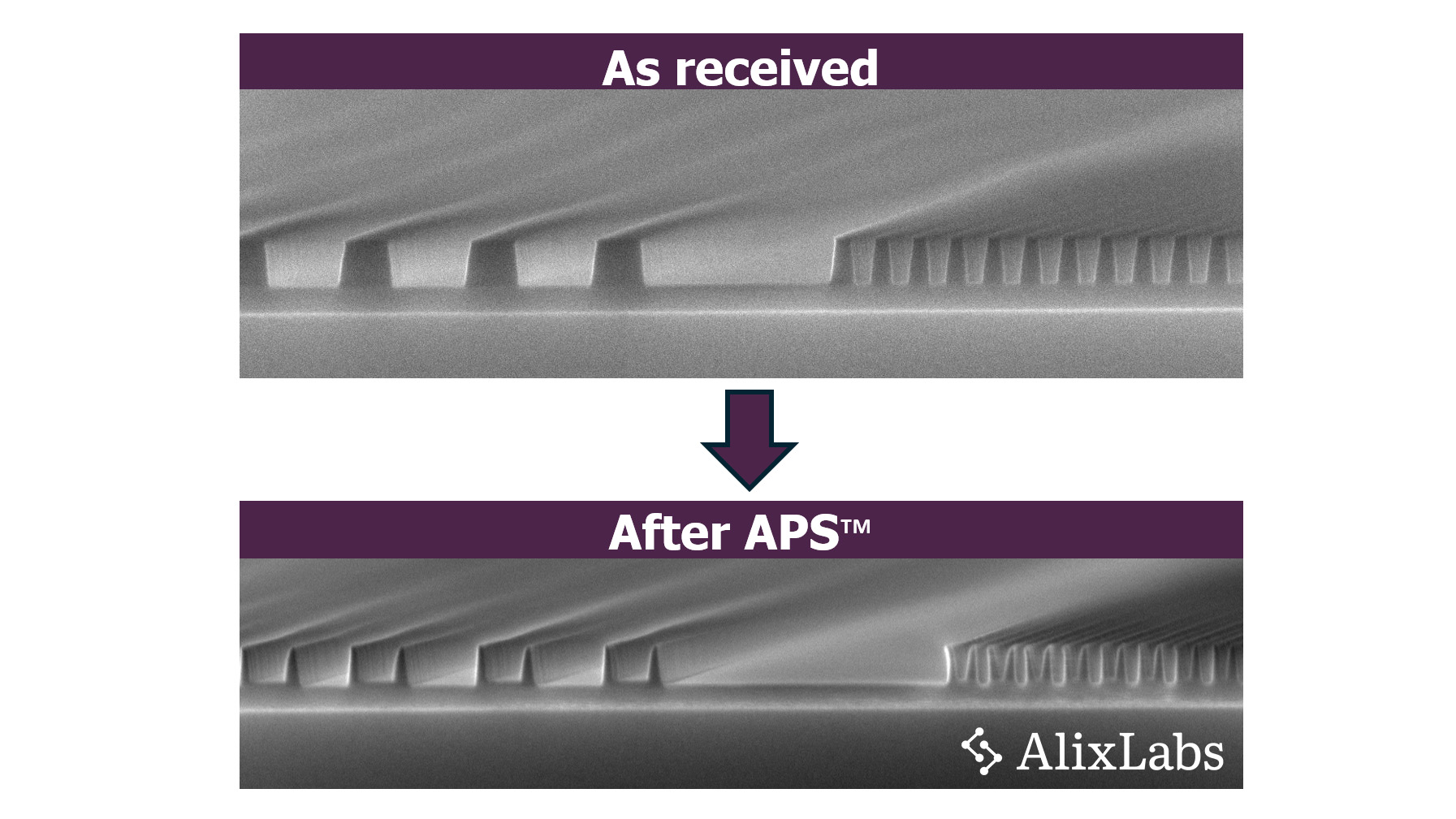
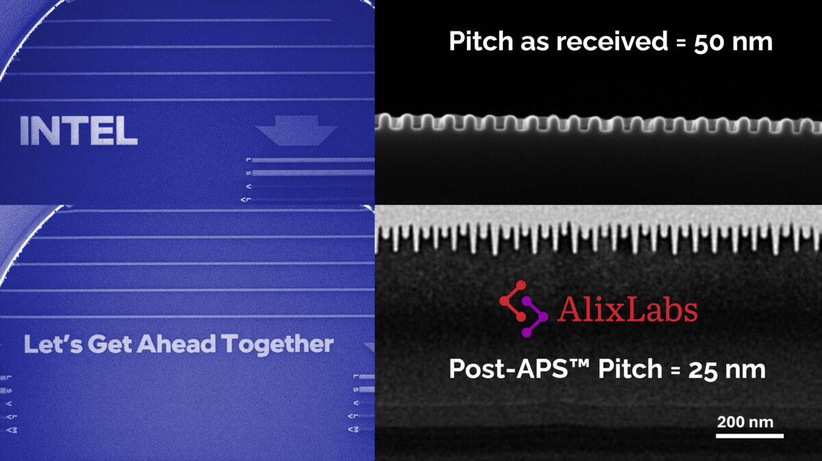
Proven on 300-millimeter wafers provided by United Microelectronics Corporation (UMC), the APS™ technology successfully halved pitch compared to current industry benchmarks. This significant advancement was achieved entirely without relying on expensive and energy-intensive Extreme Ultraviolet (EUV) lithography.
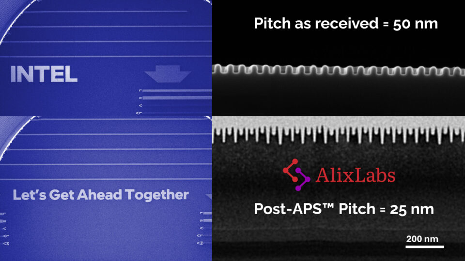
Instead, APS™ leverages advanced etching techniques that substantially enhance sustainability, drastically reducing energy consumption without compromising throughput. Previous demonstrations of the APS™ process, validated through Intel’s Test Vehicle Program[1], confirmed its potential by achieving metal pitches as small as 25 nanometers.
“Today we are sharing more proof that the APS™ process can be a game changer for leading foundries. Thanks to UMC, we have been able to verify our process on production wafers that are shipped in quantities measured in millions of wafers annually,” said Dr. Robin Athle, Principal Researcher at AlixLabs. “Our mission is to create equipment that allows companies that don’t have access to EUV tools to scale down their production to 5 nanometer and beyond. By eliminating the dependency on EUV lithography, we are offering the industry a path towards more sustainable and economically feasible high-density chip production.”
Detailed results from AlixLabs’ UMC wafer tests and further insights into APS™ technology will be presented at the 2025 CMC Conference, scheduled for April 10th in Austin, Texas. Dr. Athle’s presentation “Atomic Layer Etching Pitch Splitting (APS™): a New Alternative to Multi Patterning” will be held at 4:00 PM at the Bergstrom Ballroom in Hilton Austin Airport Hotel.
[1] https://www.alixlabs.com/2025/02/07/alixlabs-to-showcase-latest-aps-findings-at-spie-advanced-lithography-patterning/
