Swedish semiconductor startup clears technical hurdle for leading-edge process use on 300 mm wafer design.
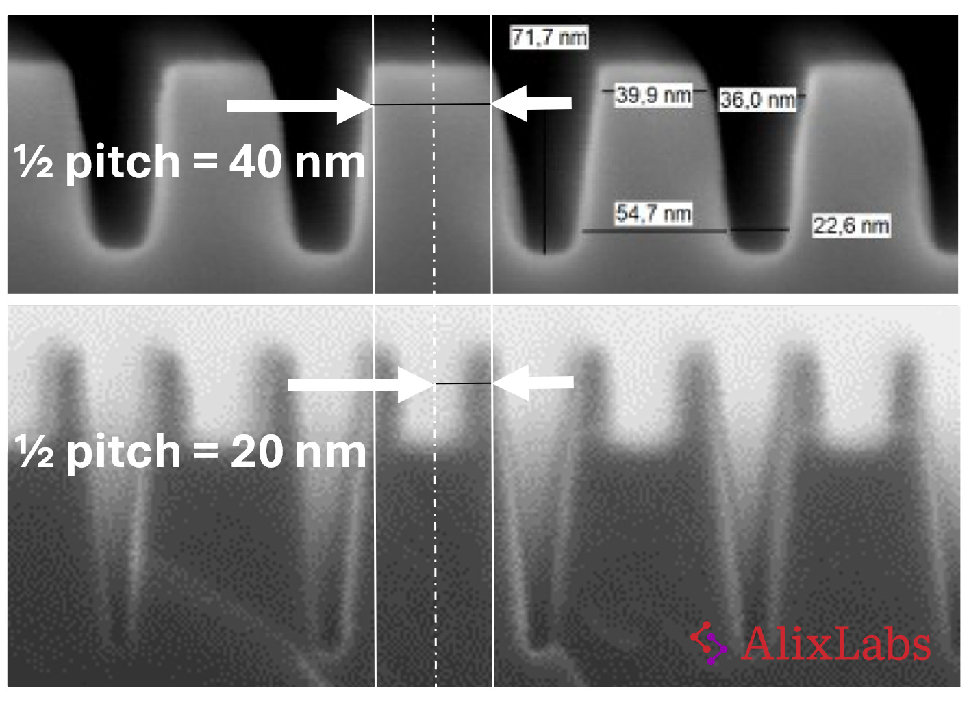
Stockholm, Sweden – September 12th, 2024 – AlixLabs AB, a Swedish semiconductor startup specializing in Atomic Layer Etching (ALE), announces that it has qualified its APS™ (ALE Pitch Splitting) process on a 300-millimeter silicon wafer design, marking one of its final steps towards commercial adoption. APS™ provides atomic-scale precision and pattern fidelity with critical dimensions below 15 nanometers for both single crystalline and amorphous silicon.
AlixLabs APS™ is designed to reduce the cost of leading-edge manufacturing, sub-7-nanometer, where feature sizes of less than 20 nanometers are required. An estimated cost saving of up to 40 percent per mask layer can be achieved with APS™ rather than relying on EUV lithography, and complex self-aligned multi patterning schemes.
“Proving that APS™ works on lithography designs on 300-millimeter wafers, is what we’ve all worked on since we founded AlixLabs in 2019,” says CEO and co-founder Dr. Jonas Sundqvist. “Not only do we aim to provide chip manufacturers wafer processing equipment that can create 20-nanometer half-pitch lines and critical dimension below 15 nanometers on silicon, we aim to do that at a lower cost and a more sustainable way than other technologies”
“We are also able to provide record breaking 3-nanometer critical dimension features on gallium phosphide (GaP) wafers today showing that APS™ can scale far into the future beyond what is needed today,” adds CTO and co-founder Dmitry Suyatin.
APS™ is positioned as an alternative to self-aligned double and quadruple patterning (SADP and SAQP). It allows for splitting dense line structures that can act as a foundation for transfer-etch into various materials such as dielectrics, metals, metal nitrides, and high-k dielectrics. The structures created with APS™ can also be used as-is for critical device features such as the fins in FinFET-type transistors due to extremely low surface damage.
AlixLabs’ goal is to supply leading semiconductor manufacturers, in both logic and memory segments. By enabling them to simplify and speed up their chip production at least fourfold for each critical mask layer by replacing four plasma wafer processing chambers in the SADP process flow with one APS™ chamber and eightfold correspondingly in SAQP. Finally, AlixLabs contributes overall to more sustainable semiconductor manufacturing.


