

Power ALE™ for GaN and SiC Power Devices
Power ALE™ Addresses the Processing Challenge in GaN and SiC Power Devices
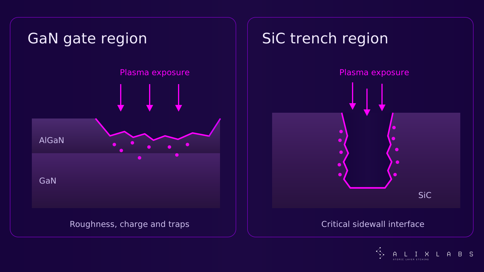
GaN and SiC are becoming increasingly important semiconductor materials for power conversion because they enable higher electric fields, faster switching and higher power densities than conventional silicon devices. However, extracting these advantages at the device level places demanding requirements on semiconductor processing.
A particular challenge is plasma etching. Reactive ion etching processes provide the etch rates and anisotropy required for semiconductor manufacturing, but they can also introduce surface roughness, lattice damage, defects, traps and fixed charge. In GaN and SiC power devices, these effects can occur at surfaces that subsequently form part of the electrically active device, thereby can directly degrade channel mobility (switching speed), off-state leakage current (off-state power dissipation), and breakdown voltage.
The problem is therefore not simply how to etch GaN or SiC. It is how to remove material with atomic-scale accuracy while preserving, or even improving, the electrical quality of the resulting surface and interface.
AlixLabs addresses this problem with Power ALE™, its application of Atomic Layer Etching to wide-bandgap power semiconductor manufacturing. Rather than positioning ALE as a replacement for every conventional plasma etch, Power ALE™ can be used where precision, selectivity, low damage and surface quality have a disproportionate impact on device performance.
GaN HEMTs Require Precise Etching Without Damaging the Channel
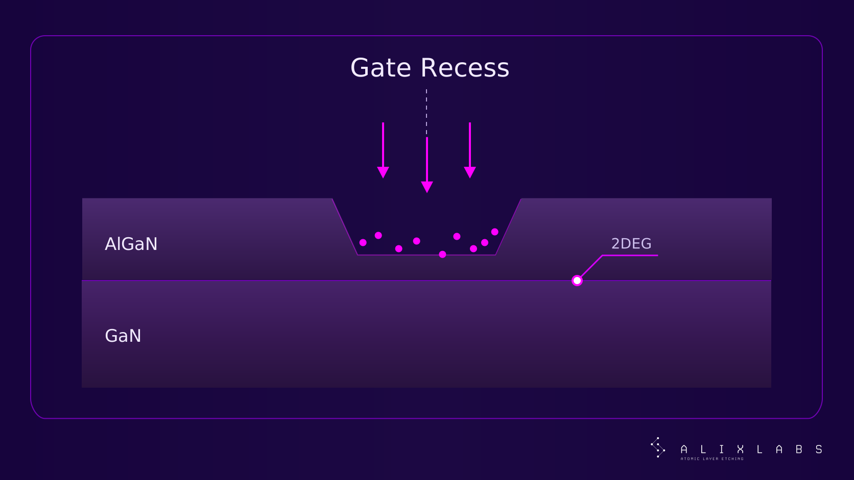
One important application is the fabrication of normally-off enhancement-mode GaN HEMTs. A conventional AlGaN/GaN HEMT forms a high-density two-dimensional electron gas (2DEG) at the AlGaN/GaN heterointerface and is normally on. For many power-electronics applications, normally-off operation is preferred for system safety and gate-control reasons.
One method of producing an enhancement-mode device is to recess the AlGaN barrier in the gate region. This makes the remaining barrier thickness a critical device parameter. Removing only a few additional nanometers can substantially change the electrostatics of the channel and therefore the threshold voltage.
Conventional RIE creates an additional problem: the recess process can damage the surface. AlixLabs’ experimental work identifies trap states, fixed charge and surface roughness as mechanisms that can reduce the effectiveness of gate control. Consequently, two nominally similar recess depths do not necessarily produce the same electrical response if the surfaces have experienced different plasma processes.
Power ALE™ approaches the recess differently. Atomic Layer Etching uses a self-limiting cyclic process in which the top atomic layer is first chemically modified, and the modified layer is subsequently removed with minimal damage caused to the sub-surface. The objective is a controlled etch-per-cycle rather than continuous material removal. This enables the AlGaN thickness to be adjusted with significantly greater precision while reducing damage to the material that remains.
AlixLabs’ GaN work shows that threshold voltage increases with recess depth, as expected from depletion of the 2DEG. More importantly, the Power ALE™-processed structures show a stronger threshold-voltage response per nanometer removed than the comparison RIE process. AlixLabs attributes the weaker response from RIE to etch-induced traps, fixed charge and surface roughness.
This makes Power ALE™ relevant not only as an etch technology but as an interface-engineering process. The objective is to obtain the required geometry while leaving an electrically better-defined surface for the subsequent gate stack.
AlixLabs is also developing ALE for GaN surface smoothing, SiNx processing and more advanced GaN structures. Its work within the EU funded ALL2GaN program includes GaN-on-SiC, D-mode and E-mode HEMTs, alternative substrates and emerging vertical and nanostructured GaN device concepts.
SiC Power Devices Benefit From ALE Sidewall Smoothing
The application in SiC power MOSFETs (trench MOSFETs) is related but different. Here, one particularly interesting use of Power ALE™ is the treatment of etched trench sidewalls.
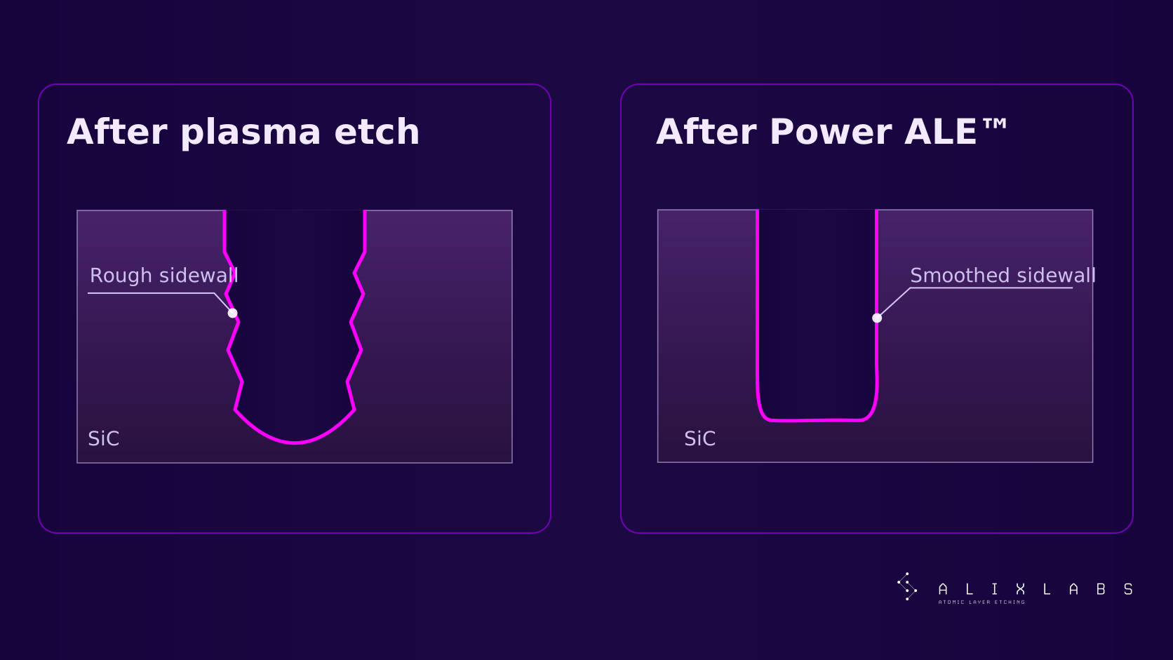
Trench structures are important in advanced SiC power devices because they can improve device geometry and utilization of the semiconductor area. However, the plasma process used to form a deep SiC trench can leave a rough and damaged sidewall. That surface can subsequently become an important part of the gate dielectric/semiconductor interface.
Using a slow atomic-scale process to perform the complete deep trench etch would not necessarily be economically attractive. AlixLabs therefore demonstrates another way of using Power ALE™: conventional plasma etching performs the high-rate material removal, followed by Power ALE™ as a precision finishing process.
The results in AlixLabs’ SiC work show a substantial reduction in sidewall roughness. The as-received trench sidewall had an Sa of approximately 0.95 nm and Sq of 1.22 nm. Two optimized ALE processes reduced Sa to approximately 0.49-0.50 nm and Sq to approximately 0.61-0.64 nm. This corresponds to roughly a 47-48 percent reduction in average sidewall roughness.
The result is important because the cross-sectional SEM analysis indicates that the improvement can be achieved with minimal impact on the overall trench profile. Power ALE™ is therefore removing or reducing nanoscale surface features rather than substantially changing the intended device geometry.
Similar surface-smoothing behavior has been demonstrated on planar material. AlixLabs reports GaN surface Rq decreasing from approximately 0.13 nm to 0.070 nm after Power ALE™ and SiC Rq decreasing from approximately 0.162 nm to 0.071 nm in the examples presented.
These measurements demonstrate the surface-engineering capability of the process. The eventual improvement in finished SiC device characteristics still needs to be established through device fabrication and electrical characterization. It is therefore appropriate to distinguish between the demonstrated reduction in roughness and the expected electrical benefits of creating a better semiconductor/dielectric interface.
Power ALE Adds Precision Where Device Performance Is Most Sensitive
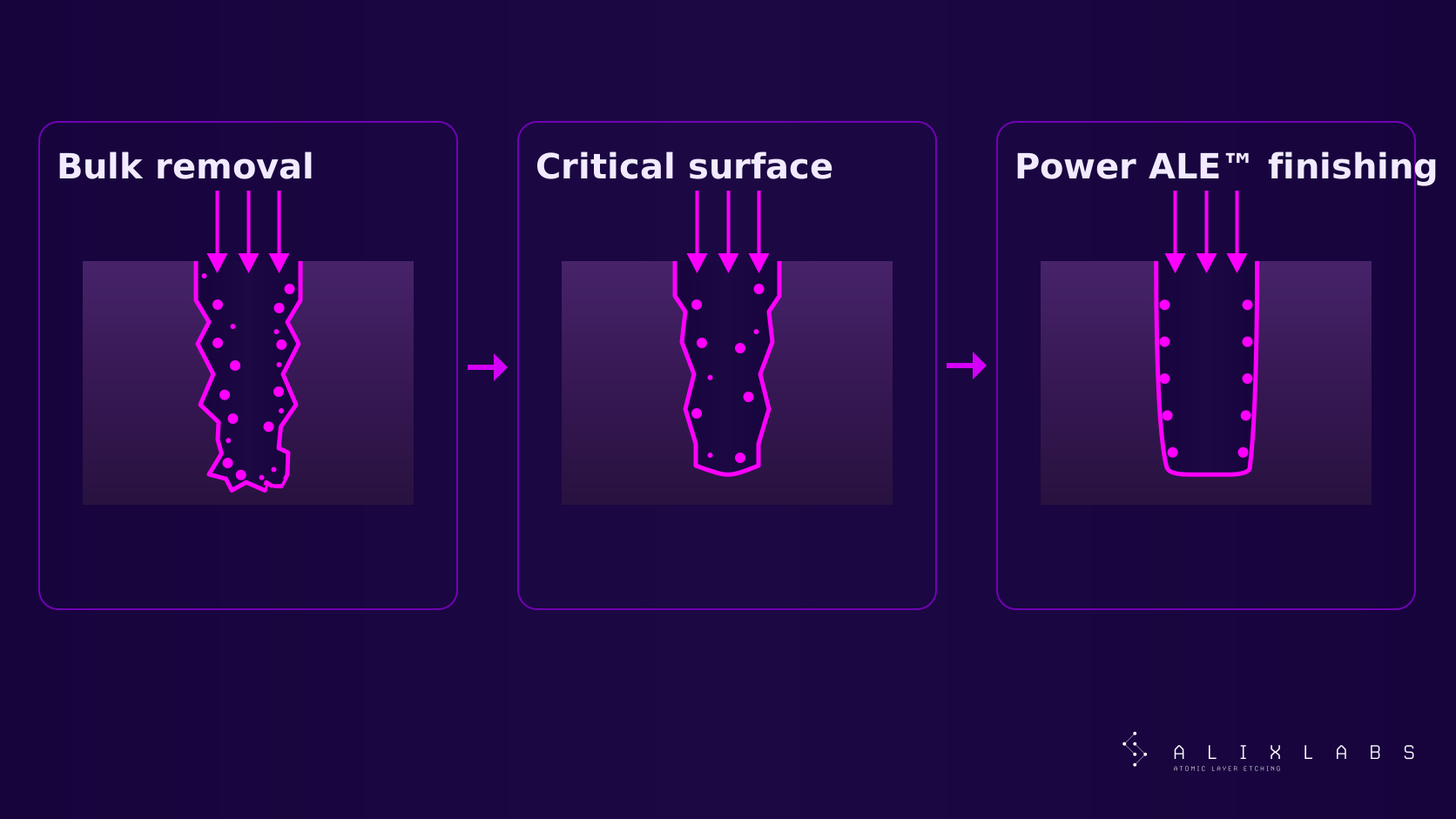
The common theme across the GaN and SiC applications is that the most important value of ALE is not necessarily its ability to remove large quantities of material. Its value is the control it provides during the final nanometers of processing.
In a GaN E-mode HEMT, those nanometers can determine the remaining AlGaN barrier thickness, the condition of the underlying surface and ultimately the threshold-voltage behavior. In a SiC trench device, Power ALE™ can modify the final sidewall surface without significantly altering the macroscopic trench geometry. In GaN epitaxy and nanostructure applications, it can also be used to prepare smoother surfaces before subsequent processing or material growth.
This suggests a complementary relationship between conventional RIE and Power ALE™. RIE provides high material-removal rates and throughput. Power ALE is introduced at the process steps where atomic-scale depth control, selectivity, low damage or surface roughness become more important than etch rate.
For a semiconductor manufacturer, the potential benefits are tighter control of critical dimensions and etch depth, reduced plasma-induced damage, smoother semiconductor surfaces and trench sidewalls, improved selectivity between device layers and a softer landing on sensitive channel materials. At the device level, these process improvements are intended to translate into more reproducible threshold voltages, improved semiconductor/dielectric interfaces, lower carrier scattering, lower OFF-state leakage current, better device uniformity and ultimately improved performance and reliability.
The significance of Power ALE™ is therefore broader than simply introducing another etch technique into GaN and SiC manufacturing. It provides a way of separating bulk material removal from the final precision processing of the electrically critical surface. Conventional plasma etching can perform fast etch; Power ALE™ can perform the last, performance-critical part of the process.
AlixLabs Power ALE Equipment Platform for SiC and GaN Processing
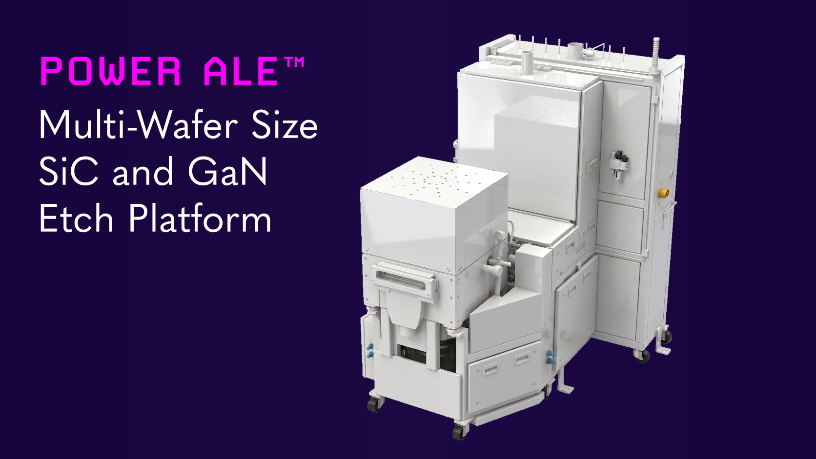
The AlixLabs Power ALE™ platform is a production-oriented plasma processing system developed for advanced wide-bandgap power semiconductors, with an initial focus on SiC and direct applicability to GaN. The platform combines Atomic Layer Etching with a semiconductor-fab-compatible hardware and software architecture designed to provide precise control of plasma conditions, surface chemistry and material removal. Its primary purpose is to address critical process steps where conventional plasma etching alone cannot provide the required combination of profile control, low damage and surface quality.
A key feature of this Power ALE™ system is its multi-wafer-size architecture. The equipment is built around a 300 mm platform while supporting 150, 200 and 300 mm wafers—corresponding to 6-, 8- and 12-inch formats. This is particularly relevant for the wide-bandgap industry, where different wafer sizes are used depending on material, device architecture and manufacturing generation. The common equipment architecture allows manufacturers to use the same fundamental process platform as production evolves between wafer sizes.
At the core of the system is a vertically configured plasma chamber combining an inductively coupled plasma (ICP) source with independently controlled wafer bias. The ICP source provides high plasma density, while the separate RF bias controls the ion energy reaching the wafer. Both RF sources support pulsed operation and synchronization. This decoupling of plasma density and ion energy control is particularly important for ALE, enabling controlled cyclic surface modification and material removal in a self-limiting manner while minimizing undesired plasma-induced damage.
Engineered for atomic-scale precision, the chamber integrates independent active thermal management across the pedestal, showerhead, walls, and lid. Substrates are held securely by mechanical clamping or an optional electrostatic chuck (ESC). Advanced yttria-coated field-replaceable liners deliver uniform plasma confinement while safeguarding internal chamber walls against aggressive plasma etch chemistry. The modular gas system isolates corrosive gas delivery from non-corrosive gases and enables sub-10 ms dosing. Combined with high-capacity pumping and automatic pressure control, the platform offers complete, decoupled control over chemistry, pressure, plasma density, ion energy, and temperature for maximum process flexibility.
The equipment is designed for automated fab operation using a production-grade load-lock and robotic wafer-handling platform. The 300 mm automation architecture can be adapted to smaller wafer formats through the appropriate wafer stage and wafer-handling configuration. This provides a common equipment path from 150 mm development and manufacturing through 200 mm production and ultimately 300 mm processing.
For SiC, Power ALE™ can support plasma etching, trench profile engineering, sidewall smoothing and surface conditioning. AlixLabs has demonstrated Power ALE™-based reduction of SiC trench sidewall roughness with minimal impact on the overall trench geometry. For GaN, the same hardware architecture can support precision GaN and AlGaN etching, E-mode HEMT gate recess, surface smoothing and preparation of sensitive semiconductor interfaces.
Power ALE™ can therefore be viewed as a multi-wafer-size, wide-bandgap plasma and Atomic Layer Etching platform: one scalable hardware architecture for 6-, 8- and 12-inch SiC and GaN processing, combining automated wafer handling with precise control of plasma, chemistry, temperature and ion energy.
Demos and inquries
For more info and demos with Power ALE™, don’t hesitate to contact us.